DIY Computer Part 5 Machine Architecture
A continuation of my participation in the amazing Nand2Tetris course, by Noam Nisan and Shimon Schocken, now running on Coursera.
Related posts:
- [DIY Computer Part 1 The NAND Gate]({% post_url 2016-03-06-diy-computer-nands %})
- [DIY Computer Part 2 The ALU]({% post_url 2016-03-12-diy-computer-alu %})
- [DIY Computer Part 3 Memory]({% post_url 2016-03-12-diy-computer-alu %})
- [DIY Computer Part 4 Machine Language]({% post_url 2016-05-23-diy-computer-ml %})
Now armed with the necessary elementary logic gates and chips, are now ready to assemble a general purpose computer. Using a finite amount of hardware, it will be capable of performing practically an infinite number of tasks (e.g. games, word processing, networking). This remarkable flexibility, the fruit of the profound invention of several mathematicians in the 1930’s, is known as the stored program.

The logic of programs is not embedded in the hardware, as was the norm for mechanical computers predating the 1930. Instead, the program code is stored and manipulated in the computer memory, just like data, becoming what is known as “software”.
The stored program formed the basis for several abstract and practical computer models, most notably the abstract universal Turing machine in 1936, and later practically implemented as the von Neumann machine in 1945.

Background reading is chapter 5 from Nisan and Schocken’s offical textbook The Elements of Computing Systems. We begin with an overview of the von Neumann architecture, highlighting the way in which the ALU interfaces with memories and registers, using buses. The memory of a von Neumann machine holds two types of information; data and instructions.
The Fetch Execute Cycle⌗
A general purpose machine, needs a way of fetching an instruction, and then executing the instruction. This cycle is then simply repeated.
Fetching
- Read the Program Counter (PC) register, for next instruction location (address).
- Read the instruction from program memory, using the above location.
- Write the instruction into the control bus of the CPU.
The value of the program counter (PC), defines the next instruction to be executed, and can be manipulated. It is common to run a program by working through its instructions sequentially (e.g. instruction 1, then 2, then 3, and so on), however, in the case of jump operations, require a way to move to a specific instruction location.
Execute
- Read the instruction code, using the control bus.
- This instruction itself contains all the details about what needs to take place (the operation to be performed, input registers or data memory locations for the operation, registers or data memory locations to be used for output).
Program Memory vs Data Memory⌗
The fetch cycle is concerned about reading instructions from program memory, where the execute cycle is concerned about reading data memory for its input and output. Given, in a von Neumann machine, there is only one memory, there is a clear problem here. How can both the fetch cycle and execute cycle share the single memory at the same time. Because the fetch state and the execute state occur at different points in time (a finite state machine in other words), a multiplexor that uses a fetch/execute bit as input (bit 15 the left most bit in the HACK), could route instruction memory for a fetch, or data memory for an execute.
Input and Output⌗
Computers interact with their external environments using input and output (I/O) devices, such as a display, keyboard, printer, scanner, network interface cards, optical drives, microphone and many more, each of them requiring unique machinery and engineering knowledge. A general purpose computer does not need to concern itself with the specifics of these various devices, as these devices are made to look exactly the same to the computer, using an elegant scheme known as memory mapped I/O.
Simply, each device represents itself in a memory segment that is accessable to the CPU. Each device is allocated an exclusive area in memory, becoming it’s very own memory map. In the case of an input device such as a mouse or keyboard, the memory map is made to continously reflect the state of the device, or in the case of an output device such as a display or speaker, the memory map is made to continuously drive the physical state of the device. Awesome!
To implement such a feat, the API to the memory chip takes in a 16-bit input (to potentially store), a load bit indicating if the data should be stored, and a 15-bit address that points to one of the 16-bit slots within the memory (which could be from a chip such as RAM or an I/O device). The memory chip has a 16-bit output of the slot that was read. To provide a single unifed address space across both data memory, and a number of I/O devices (such as a screen and keyboard), we need some bit patterns that uniquely identify when what device should be mapped. Nisan and Schocken have elegantly designed the “hack” implementation, and this pattern emerges in the 15-bit addressing scheme through bits 14 and 13. You’ll need to really wrap your head around each bit in the Hack machine language specification (in Nisan and Schocken textbook The Elements of Computing Systems), so the CPU you design is capable of running Hack compliant instructions.

| Address range | Bit 14 | Bit 13 | Destination chip |
|---|---|---|---|
| 0-16383 | 0 | 0 or 1 | Data memory (RAM64K) |
| 16384-24575 | 1 | 0 | Screen |
| 24576 | 1 | 1 | Keyboard |
Given two bits 14 and 13 from the address, we can demultiplex and multiplex between the three chips (RAM64K, Screen and Keyboard), automatically for the user, via a consistent API of inputs and output, or in other words, provide memory mapped I/O.

Note the keyboard chip never receives input, as keyboards only ever produce output.
CPU Implementation⌗
Finally we delve into wiring up the CPU itself, by leveraging the high-level chips we have previously built, including the A and D registers, the ALU, a several elementary logic gates such as AND’s and OR’s. Designing this chip takes time, be patient and don’t give up, its hugely rewarding to see your very own CPU pass all the test cases in the hardware simulator. Again Nisan and Schocken cleverly guide you down a path, by suggesting an implementation with just the data and address buses wired up, but totally leave the control logic up to you to design. It took me several hours to come up with the following, with lots of head scratching and sheets of paper…
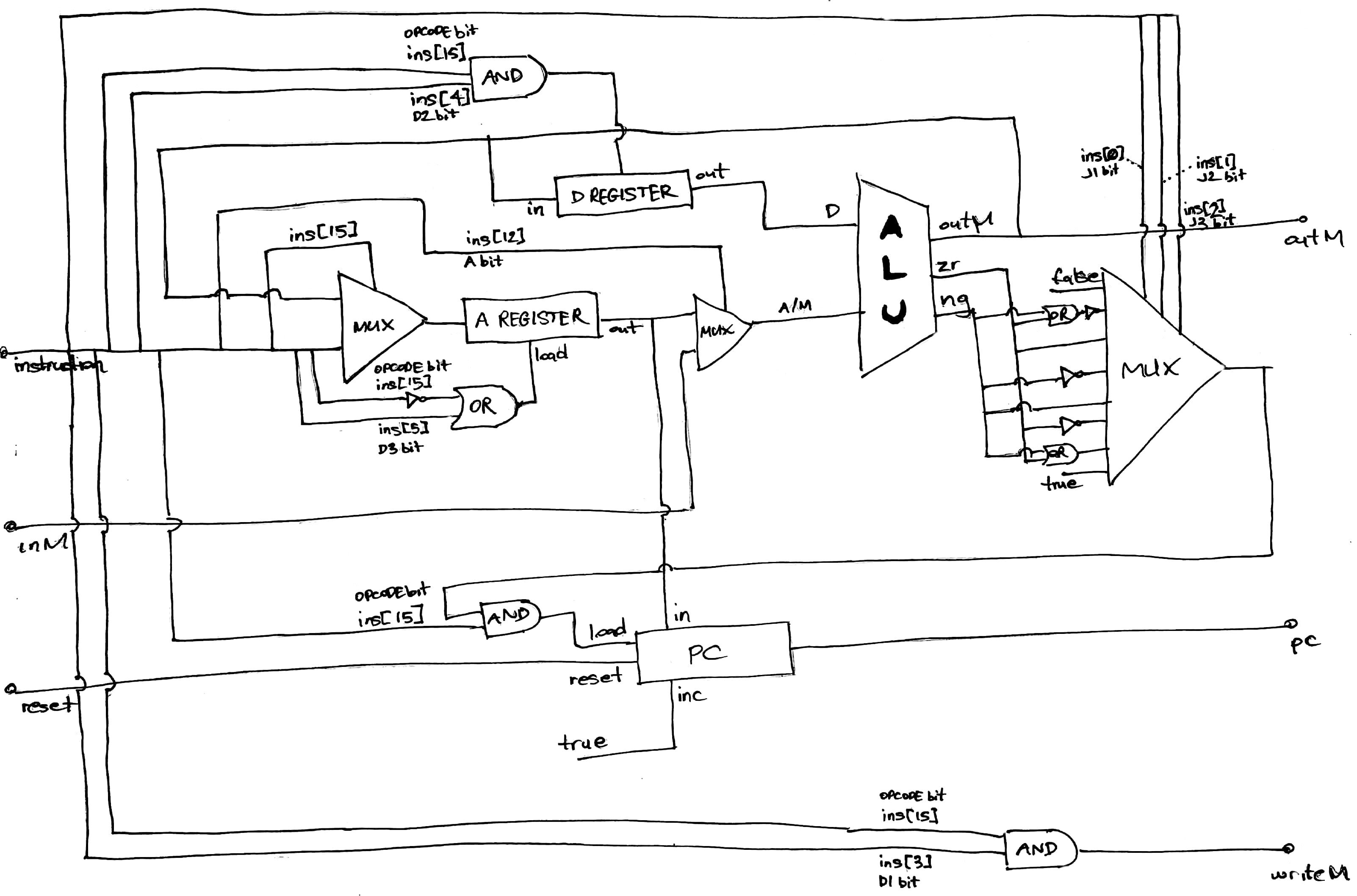
You’ll need to really wrap your head around each bit in the Hack machine language specification (in Nisan and Schocken textbook The Elements of Computing Systems), so the CPU is capable of running Hack compliant instructions.