This material is based on the high quality build your own CPU guide by Ben Eater. Ben cites the SAP-1 CPU architecture as the design inspiration for the CPU, which originated from the book Digital Computer Electonics by Albert Paul Malvino.
The SAP (Simple As Possible) computer has been designed for you, the beginner. Its purpose, to introduce the crucial ideas behind a CPUs operation without burying you in unnecessary detail.
- Architecture
- General Electonics
- The clock
- The registers
- Arithmetic and Logic Unit (ALU)
- Program Counter (PC)
- Output register
- Handy resources
Architecture
The SAP-1 defines a number of logical CPU modules which are capable of integrating to form a working CPU and ultimately computer.
Each module can be thought of as defining an API; they take inputs and they produce outputs.
For example, the PC (Program Counter) module, defines 3 input flags:
COif set, will output current counter value to the busJif set, will load the current address of the bus and set it as the counterCEif set, will enable the counter which will increment on each rising clock pulse
General Electonics
Dirty power
Using an oscilloscope will observe the transition from low to high is rather dirty. To overcome this, the data sheet recommends dropping in a 0.01uF capacitor between pin 5 and ground. In addition placing a 0.1uF capacitor across the positve and negative power pins. When the transistors state change, they immediately attempt to pull in as much current as they can to drive from low to high. At the nano second scale on the oscilloscope, can see this results in a slight lag in pulling the needed current, and also results in a voltage spike/overshoot. To feed this state transition with the needed current, filling up a capacitor (in this case, a 0.1uF across positve and negative pins) will provide an immediate pool of current for use, resulting in a faster low to high, and consequently less of an overshoot/spike.
Resistors
Measured in ohms. Resistors commonly come in 4 and 5 band variations. A 4 band simply skips out of the 3rd significant digit.
- 1st significant digit
- 2nd significant digit
- 3rd significant digit
- multiplier
- tolerance
Capacitors
Measured in pico farads.
Ceramic caps, due to tiny print real-estate use a 3 digit numeric code, such as 104. A 1st and 2nd significant digit, followed by a multiplier. Therefore a 104 = 100,000pF = 100nf = 0.1uF
Latch vs flip flop
Conceptually similar. A latch is immediately influenced by its inputs. A flip flop on the other hand is not.
D flip flop
Has a single data input D, and a clock input. It will store the input state D, at the time of the rising edge of the clock pulse.
The timing diagram helps drive this home:
The clock
2020-07-12
First up to tackle the clock, the backbone of synchronising all digital operations within the CPU. The classic 555 timer IC has been selected, due to its versatility.
The clock will provide an adjustable speed (1Hz upto 200Hz), and a handy debugging push button manual mode to advance a single clock cycle.
The 555 essentially contain a couple of comparators which feed into an SR latch. The first trigger comparator is set to a high voltage of 1.67v, and the second threshold comparator set to a low voltage of 3.33v. When the 3.3v threshold is hit, a discharge transistor is enabled, which drains the capacitor (external to the 555 IC). This capacitor will continually drain and fill, based on this relationship. The drain and fill (duty cycle) rates of the capacitor can be controlled by resistors.
The timing period in seconds can be calculated as 0.693 (Ra + 2Rb) C
For example a 555 configured with an Ra of 1K ohms, Rb of 100K ohms, and a 1uF capacitor:
0.693 (1000 + 2 * 100000) 0.000001
0.139293 seconds
555 timer modes:
- Astable generates a constant stream of square waves
- Monostable provides two states, one stable (push button controlled), and one unstable variable stream of square waves
- Bistable, aka a flip flop, stable in both states, output high and output low
The registers
2020-08-22
Registers are how a CPU persists data. Registers are cool, because they can store (latch) and/or output their 8-bits of state conditionally, using the load and enable pins.
Given the SAP-1 supports 8-bits, this CPU will feature 3 8-bit registers A, B and IR. The A and B registers are general purpose. The IR, or instruction register, will keep track of the current instruction being executed.
A first attempt at building a register, one might reach for 8 D flip flops to store the state of each input bit.
This will unconditionally store the state. We still need to figre out a way to only conditionally store the input data (from a common bus backbone) only when the load bit is enabled.
To prevent all the registers sourcing and sinking their inputs and outputs onto the common 8-bit bus which interconnects them, there needs to be a way to physically disconnect the 8 input pins and/or the 8 output pins to each register.
This is where tri-state logic gates come to the rescue. In tri-state logic, a third NULL state is introduced. Outputs can now be high, low or nothing.
The 74LS245 provides 8 tri-state buffers, that can be enabled or disabled with an overall enable pin.
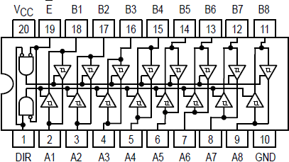
Here Ben presents an interesting decision point. To either keep using discrete logic gates (hardcore purist) or shortcut to using pre-fabed chips such as the 74LS173, which includes four 1-bit (aka 4-bit) D register including tri-state buffered output!
Fantastic, this provides all the primitive building blocks to conditionally source 8-bits of input from the bus, and to conditionally sink 8-bits of output to the bus.
While its doable to build these registers by hand using primitive logic gates, it would take a serious amount of space and chips. I’m going with the shortcut option, which will use 2 of the 74LS173 so we can store 8 individual bits. A nice design option, Ben suggests hardwiring the tri-state output to true, so we can wire up LED’s to always visualise the state within each register. As a result, each LED ouput leg now must be wired through a tri-state buffer, and will use the 74LS245 which provides 8 tri-state buffers in a single chip.
Each of the 3 registers (A, B and IC) will occupy a single breadboard.
The API of each register module can be conceptualised as follows.
Inputs:
- RESET: completely resets the state of the d flip flops.
- NOLOAD: when low, will latch the state of the bus
- DISABLE: when low, will output 8-bit register value to bus
- CLOCK: signals that the register should operate
- BUS: the common 8-bit bus
Outputs:
- BUS: the common 8-bit bus
This may seem odd, as the bus can act as both an input and an output to the register module.
Arithmetic and Logic Unit (ALU)
Defines the logic that makes it possible to add, substract and multiply binary number representations together. It can additionally offer boolean logic operations such as AND, OR, XOR and so on. Evaluating two binary inputs together, and spitting out the result.
In a nutshell the ALU is what makes it possible to perform computations on binary operands.
Design
The API of the SAP ALU looks like this.
Inputs:
- A register: 8 bits
- B register: 8 bits
- Subtract mode: 1 bit
- Output enabled (EO): 1 bit
Outputs:
- Bus: 8 bits
Implementation
Sticking with primative logic chips, Ben suggests:
- Daisy chaining two 74LS283 (4-bit adder) together, to support 8-bit representations. Interface of nifty little 16-pin chips:
- A1-4: first 4 bits of A register
- B1-4: first 4 bits of B register
- Σ1-4: the addition result
- C0,C4: carry out, and carry in, to support cascading chips together.
- A 74LS86 (8 XOR gates), to negate the B register only when the subtract bit is set.
- A 74LS245 (tri-state buffers) to conditionally output result to the bus, only if the output enabled (EO) bit is set.
Design for a primitive ALU that can add and subtract binary numbers:

Tri-state buffers allow for ALU output to be conditionally output on the common bus lines:

Representing negative numbers - signing bit, 1’s and 2’s complement
How does a CPU actually represent numbers.
We feable humans work naturally with base 10, and the CPU like things as base 2.
A first attempt might be to whack a signing bit on the front, to represent if the number is positive or negative.
For example the number 5 on an 4-bit CPU might look like this:
8  4  2  1
0  1  0  1
Using the far most left bit as the signing bit, negative 5 would be:
8  4  2  1
1  1  0  1
Now the problem. How does doing basic arithmetic like adding play out here?
Adding postive 5 with negative 5:
 0101 +
 1101
 ----
10010
10010 becomes 0010 as the left most 5th bit gets truncated in a 4-bit representation.
0010 is postive 2.
5 - 5 = 2
This is the problem.
Some clever people meditated on this problem and devised an elegant representation called 1’s complement.
Ones complement
Negative numbers are represented by the inverse of the binary representation of its corresponding positive number.
1001 (-6)
1010 (-5)
1011 (-4)
1100 (-3)
1101 (-2)
1110 (-1)
1111 (-0)
0000 (0)
0001 (1)
0010 (2)
0011 (3)
0100 (4)
0101 (5)
0110 (6)
Let’s see if adding works better, than using a simple signing bit:
0101 (5) +
1010 (-5)
----
1111 (0)
Nice. Another test:
 0110 (6) +
 1101 (-2)
 ----
X0011 (3)
Close, just off by one. In practice the truncated 1 could be subtracted from the right-most bit, known as end around borrow. This is a complexity when working with ones complement.
Also what’s with the -0 too!?
Two complement
Overcomes the dags of ones complement. The representation is just ones complement without the -0.
1001 (-7)
1010 (-6)
1011 (-5)
1100 (-4)
1101 (-3)
1110 (-2)
1111 (-1)
0000 (0)
0001 (1)
0010 (2)
0011 (3)
0100 (4)
0101 (5)
0110 (6)
Factoid: In twos complement when adding an integer with its negative (ex: 5 + -5) each addition operation results in 2 (i.e. two 1 bits added). Hence the name twos complement.
One difficulty arises when working with twos complement. Deducing the negative representation of a positive, is no longer simply an invert operation like in ones complement.
Example: given the number 5 0101, what is -5 in two complement?
Luckily there is a simple procedure; invert the bits, and add one.
0101 is 5
1010 invert each bit (ones complement)
1011 then add 1 (twos complement)
Program Counter (PC)
This module provides a 4-bit binary counter.
This will implement the heart of the theoretical turing machine, enabling the computer to march forward one instruction per clock cycle. Welcome to JK flip flops.
What’s a JK flip flop anyway?
Recall a the SR latch, was driven by its S (set) and R (reset) inputs. Well a latch that can persist its state, regardless of its inputs, often using a 3rd load input to toggle this behavior.
A JK flip flop is refinement of the SR flip flop, in that it overcomes the dredged scenario when both inputs are set to true. This is a condition that is normally undefined in the case of an SR flip flop.
By daisy chaining a series of JK flip flops together (known as halving) can effectively half the clock speed at each step, the least significant bit (LSB) will increment at 4 times the rate of the most significant bit (MSB).
The main worker chip to make this happen will be the 74LS161 a 4-bit synchronous binary counter.
The chip features some handy functionality, such as the ability to load a 4-bit value and set it as the current count and an enable bit to pause counting.
One missing feature on the counter chip, that is needed, is the ability to disable output of the current counter value to the bus. This will prevent the counter module from poluting the shared 8-bit bus, to only when its output is needed. As for the other modules, to achieve this conditional output, the 4-bits of output from the counter will flow through a tri-state buffer 74LS245 chip.
PC module problem 1: counter clearing
The 74LS163 data sheet shows that drawing pin 1 low is designed to clear the state of the counter. Ben did not seem to hook this up in his video walkthrough, but I found not doing this to be problematic (i.e. the chip would basically reset each clock pulse). After connecting pin 1 to 5V, the counter started to behave itself.
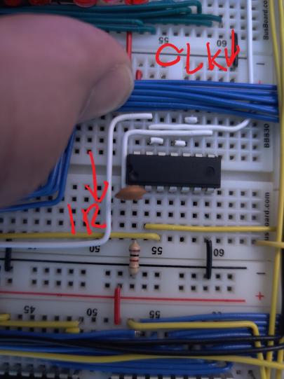
PC module problem 2: dirty clock signal
In practice making the program counter module had hurdles; the clock for some reason was generating a double spike which I traced back to the RC (resistor capacitor) circuit that was being used as an edge detector on the RAM module. I didn’t notice the problem until the binary counter chip on the PC, which was just flashing a binary 1 (i.e. 0001) every clock pulse. If I disconnected the clock from the RAM module however, boom, the binary counter would function as expected. Luckily Alex Roetter on the forums posted he experienced a similar issue and suggested hooking up two unused NAND gates near the RC circuit to make a rudimentary diode, in-turn preventing backflow from the edge detector corrupting the shared clock signal.
First recall the truth table for a NAND gate:
| A | B | out |
|---|---|---|
| 0 | 0 | 1 |
| 0 | 1 | 1 |
| 1 | 0 | 1 |
| 1 | 1 | 0 |
Using two NAND gates can run the clock (CLK) all the way though so it functionally produces the same output as the original input. On the surface this may appear to be pointless, the benefit however is that no feedback will be able to flow backwards through the NAND’s, prevent the nasty double spiking feedback on the (common) clock line from the RC edge detector circuit on the RAM module:
| CLK in | 5V in | 1st NAND out (2nd NAND in) | 5V in (2nd NAND in) | 2nd NAND out |
|---|---|---|---|---|
| 1 | 1 | 0 | 1 | 1 |
| 0 | 1 | 1 | 1 | 0 |
Alternatively (avoid having to tie a 5V as input) could do this:
| CLK in | CLK in | 1st NAND out (2nd NAND in) | 1st NAND out (2nd NAND in) | 2nd NAND out |
|---|---|---|---|---|
| 1 | 1 | 0 | 0 | 1 |
| 0 | 0 | 1 | 1 | 0 |
As per the above truth table, here’s a photo of how to run the clock through the top 2 NAND gates on the 74LS00 chip on the RAM module:
Output register
Instead of just outputting straight binary signals, Ben steps up the game by wiring in a binary-to-decimal decoder circuit. In a nutshell the circuit will translate 8 bits of binary to its corresponding decimal value on series of 7 segment LED displays. AWESOME!
SSD (seven segment displays) are heaps of fun and often found in lots of devices such as microwaves. I purchased a bag of bright green (Gallium Phosphide Green) Kingbright SC56-11GWA common cathode 7-segment displays, which my computer will use to output upto 3 decimal digits.
I imagined this would involve quite a bit of mapping logic (e.g. 00000001 to turn on the 2 RHS vertical bars on the 7 segment display, 00000010 needs to turn on 5 segments the 3 horizontal bars and 2 vertical bars, and so on). Enter PROM’s (programmable read-only memory). Using an EEPROM can write an arbitrary data bits to addresses, and it will remember what you set forever.
Given a EEPROM needs to be initialised somehow, EPROM’s were invented, Erasable PROM’s. EPROM’s are typically set and erased with exposure to ultra-violet light. Not so convenient or robust. EPROM’s were eventually superseded by EEPROM’s, Electrically Erasable PROM’s. EEPROM’s can conveniently be writen using a circuit, i.e. you set the address you wish to modify, the data input bits you want to place at the address, and a rising edge clock pulse to make it all happen. EEPROM programmers are a thing.
Ben shows how to make your very own versatile EEPROM programmer using an Arduino Nano.
We can then essentially write up some C code to store all the binary to 7-segment display mapping values, and using a loop smash then into an EEPROM chip.
Arduino Nano EEPROM programmer
The nano is an amazing little form factor that conveniently can plug straight into a breadboard - it can power the breadboard using the 5v that already comes in over the USB serial interface.
The target EEPROM chip I’m using is the AT28C64B. The simpler AT28C16 was suggested but good luck getting one of those. Good design, the pinout of the most capable chips (such as the 64) have similar pinouts, making it easy to chop and change.
The AT28C16 is a 16K memory organized as 2,048 words by 8 bits. The device is manufactured with Atmel’s reliable nonvolatile CMOS technology.
It comes as a 24 pin SOIC chip, noteworthy pins:
- A0-10: 11 pins uses to represent the current address slot (one of the 2,048 slots)
- I/O0-7: 8 pins to repsent either the byte going in or out of the selected slot
- Page 3 of the datasheet explains the various modes (read, byte write, data polling, write protection, chip clear)
- In a nutshell the !CE (chip enable), !OE (output enable) and !WE (write enable) pins are the main levers to pull
OK, so the Arduino Nano has 10 data pins (assuming you want to use the USB serial interface, which takes a few).
To drive the AT28C16 EEPROM are going to need 11 (address pins) + 8 (data pins) + 3 (mode pins) = 22 pins
Damn. What now?
Well it turns out lots of projects that use the nano need more than 10 pins and this problem has been solved by great minds a long time ago.
Enter SHIFT REGISTERS.
A shift register is a type of digital circuit using a cascade of flip-flops where the output of one flip-flop is connected to the input of the next. They share a single clock signal, which causes the data stored in the system to shift from one location to the next. By connecting the last flip-flop back to the first, the data can cycle within the shifters for extended periods, and in this form they were used as a form of computer memory.
In a nutshell using only 3 pins from the Arduino Nano to the shift register, pin 14 SER (serial data), pin 11 the SRCLK (shift register clock - to clock the bits along) and pin 12 the RCLK (register clock to indicate all bits are neated loaded - output it all in one burst), the Arduino Nano can clock in individual bits into 2 shift registers, in this case a pair of daisy chained 74HC595. Once the bits are neatly clocked in, they can then be read into the EEPROM.
- Arduino D2 -> data (pin 14)
- Arduino D3 -> shift register clock (pin 11)
- Arduino D4 -> storage register clock (pin 12)
Testing the Arduino Nano EEPROM programmer bolstered with a couple of shift registers:

Binary to decimal 7-segment decoder
Now we’re armed with a handy EEPROM programmer, its time to burn a ROM.
There many ways to load the mapping bits into the ROM. It all hinges on how you plan to wire the bus to the EEPROM, and the EEPROM to the 7-segment display. As long as everything is wired consistently fill your boots. One possible mapping scheme is as follows for a common cathode display. For common anode, flip the bits.
*dp = decimal point on the 7-segment display
   a
  ---
f| g |b
  ---
e|   |c
  ---
   d
| 0d | dp | a | b | c | d | e | f | g | 0x |
|---|---|---|---|---|---|---|---|---|---|
| 0 | 0 | 1 | 1 | 1 | 1 | 1 | 1 | 0 | 7e |
| 1 | 0 | 0 | 1 | 1 | 0 | 0 | 0 | 0 | 30 |
| 2 | 0 | 1 | 1 | 0 | 1 | 1 | 0 | 1 | 6d |
| 3 | 0 | 1 | 1 | 1 | 1 | 0 | 0 | 1 | 79 |
| 4 | 0 | 0 | 1 | 1 | 0 | 0 | 1 | 1 | 33 |
| 5 | 0 | 1 | 0 | 1 | 1 | 0 | 1 | 1 | 5b |
| 6 | 0 | 1 | 0 | 1 | 1 | 1 | 1 | 1 | 5f |
| 7 | 0 | 1 | 1 | 1 | 0 | 0 | 0 | 0 | 70 |
| 8 | 0 | 1 | 1 | 1 | 1 | 1 | 1 | 1 | 7f |
| 9 | 0 | 1 | 1 | 1 | 1 | 0 | 1 | 1 | 7b |
Notes:
- The
gpin being the represented by least significant bit (LSB) from the ROM output - The
dppin being the represented by most significant bit (MSB) from the ROM output
Multiplexing four 7-segment displays with a single EEPROM
The is a great optimisation which saves having to use several EEPROMS to represent each digit. This is awesome, because EEPROMS are big and expensive. In addition, this approach just feels minimal, less wasteful in terms wiring, energy usage.
For example, think about how you might display the number 123 (0b01111011).
A top down approach is to think about the end result you desire and work backwards from there. In this case, three separate 7-segment displays should act as follows when 01111011 (123) is the input:
   a         a         a
            ---       ---
f  g |b   f  g |b   f  g |b
            ---       ---
e    |c   e|    c   e    |c
            ---       ---
   d         d         d
The brute force approach is to use hook each of the three 7-segment displays up to it own EEPROM. So when the bits 01111011 come in, EEPROM 1 instructs a 3 to be displayed on its 7-segment, EEPROM 2 instructs a 2 to be displayed on its 7-segment and EEPROM 3 instructs a 1 to be displayed on its 7-segment. Thats allot of EEPROMS :(
Given the AT28C64B can store 64KB (8K * 8bits) we have plenty of storage.
The problem? How can we better make use of all the storage of a single EEPROM?
Enter the multiplexor approach. A primitive multiplexor, often used in networking, is great for maximising the use of a single physical connection. For example, encoding the value 101 (5) from one chip to another needs three connections for each bit right. Not with a mux, using a single connection which paired with a clock the mux can process each bit in serial, first the 1, then the 0, then the 1. On the other end of the connection a demux clocked at the same rate can process each bit, load them into dedicated connections.
With the mux mindset this multi-digit 7-segment display circuit needs to somehow:
- Activate only one 7-segment display at a time (e.g., the ones place digit, then the tens place, then the hundreds place)
- Use a single EEPROM
- Depending on what digit is active, read from a dedicated region in the EEPROM (e.g. mapping data for the ones place, the tens place, the hundreds place)
- The region specific mappings are only concerned with rendering their digit, for example to display 123, the ones digit needs only to care about making a 3, the tens digit a 2 and the hundreds digit a 1.
Given:
- A dedicated clock (555)
- A 2-bit binary counter (two daisy chain JK flip flops)
- A demultiplexor to tranlate the 2-bit counter to 4 dedicated connections
Can:
- Dynamically set the correct EEPROM memory region to read from by setting the most-significant (high) address bits to the 2-bit binary counter output
- Conditionally activate the corresponding 7-segment digit by connecting its common cathode leg to a dedicated output connection from the demultiplexor
- Set the frequency of the dedicated clock fast enough so it appears that all four digits are being displayed at the same time.
In affect multiplexing the display of the four digits, using only one EEPROM.